laser systems for processing of large substrates up to 1,2 m x 2 m. We are using a selve developed stiff core design instead of heavy granate and high dynamic and high precision linear stages (x, y and z as option). We also provide online high precision scribe and edge detection and for position correction of the laser spot with up to 700 mm / s
For thin-film photovoltaic modulen and for wafer based silicon solar cells

Stand alone laser scriber für ambient air for > 140 mm x 140 mm working ares with vision system for P1, P2, P3, LED and contact exposure

Laser system for glove box.
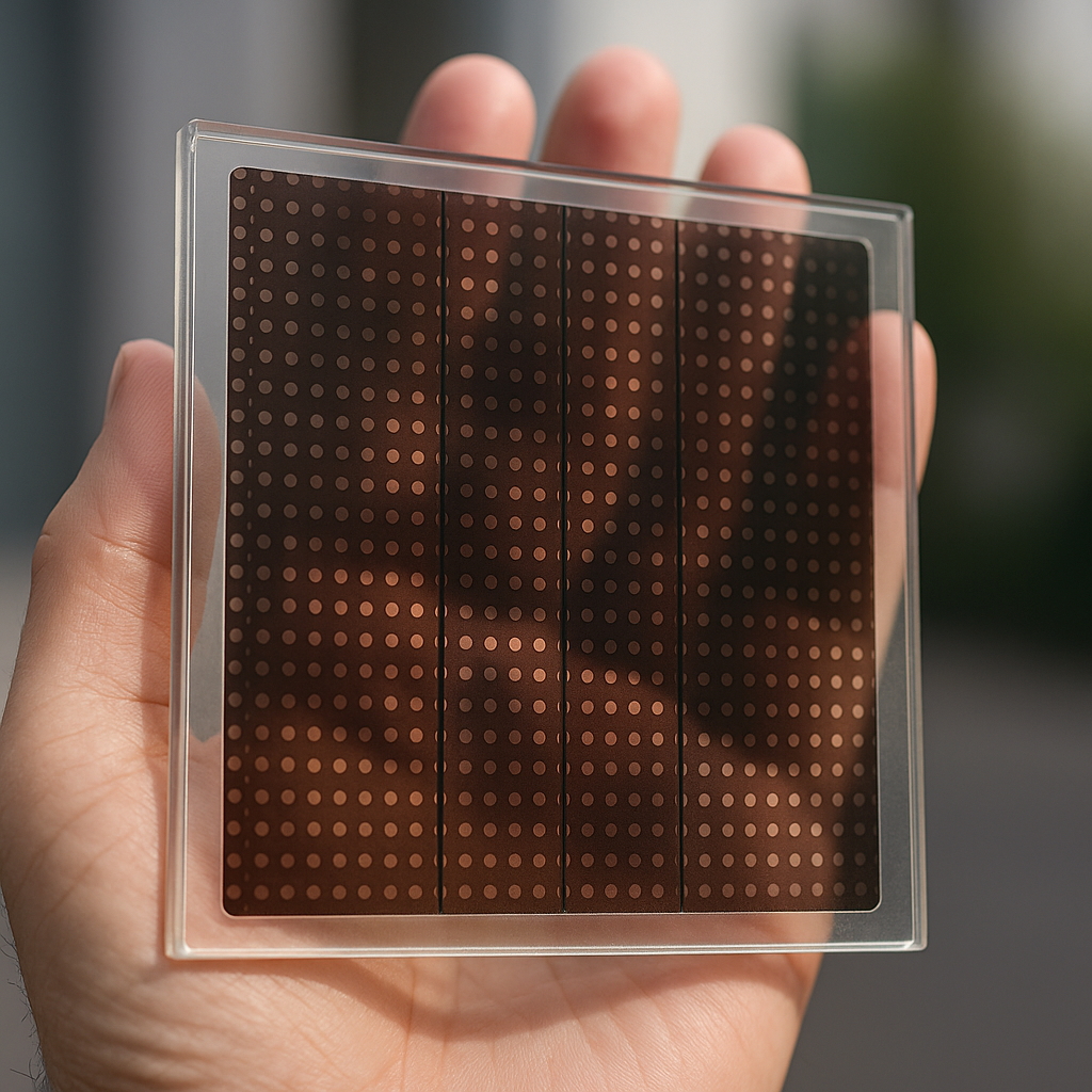
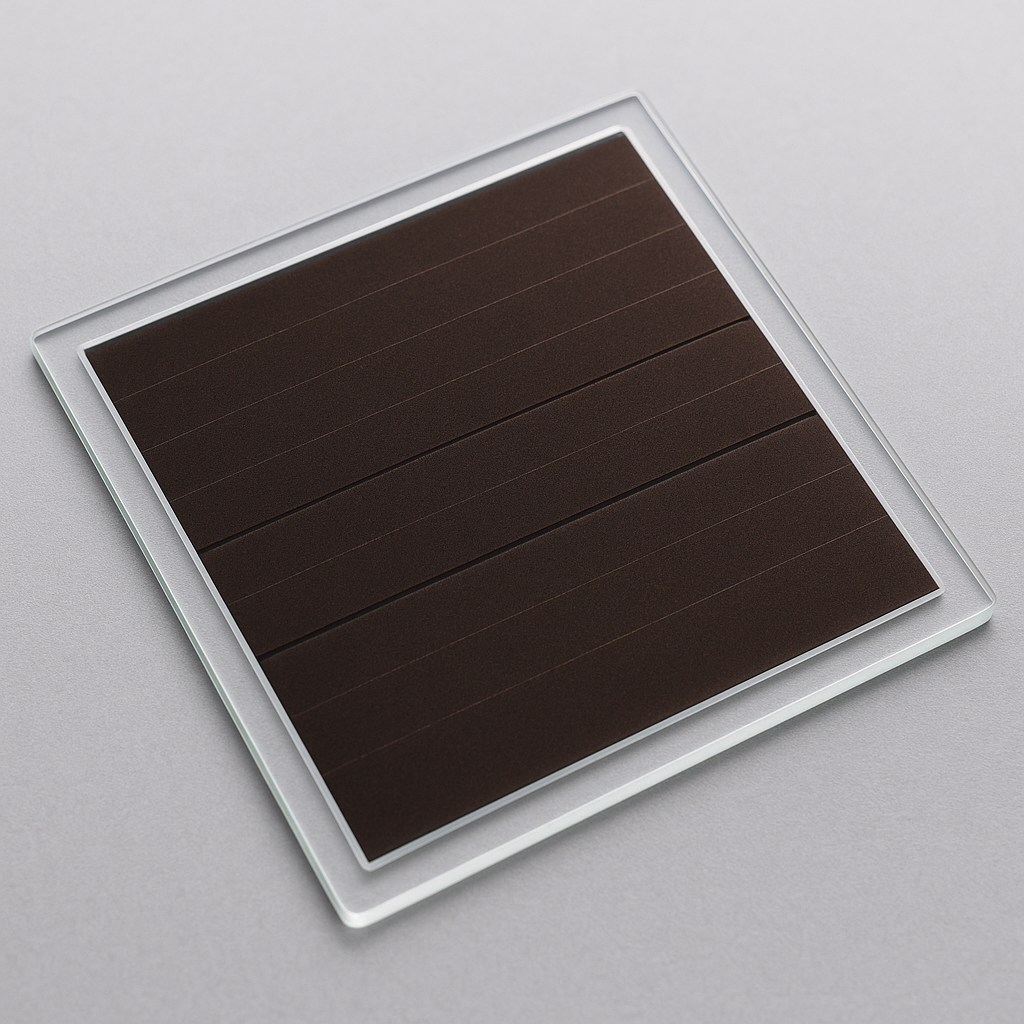
For thin-film photovoltaic modulen
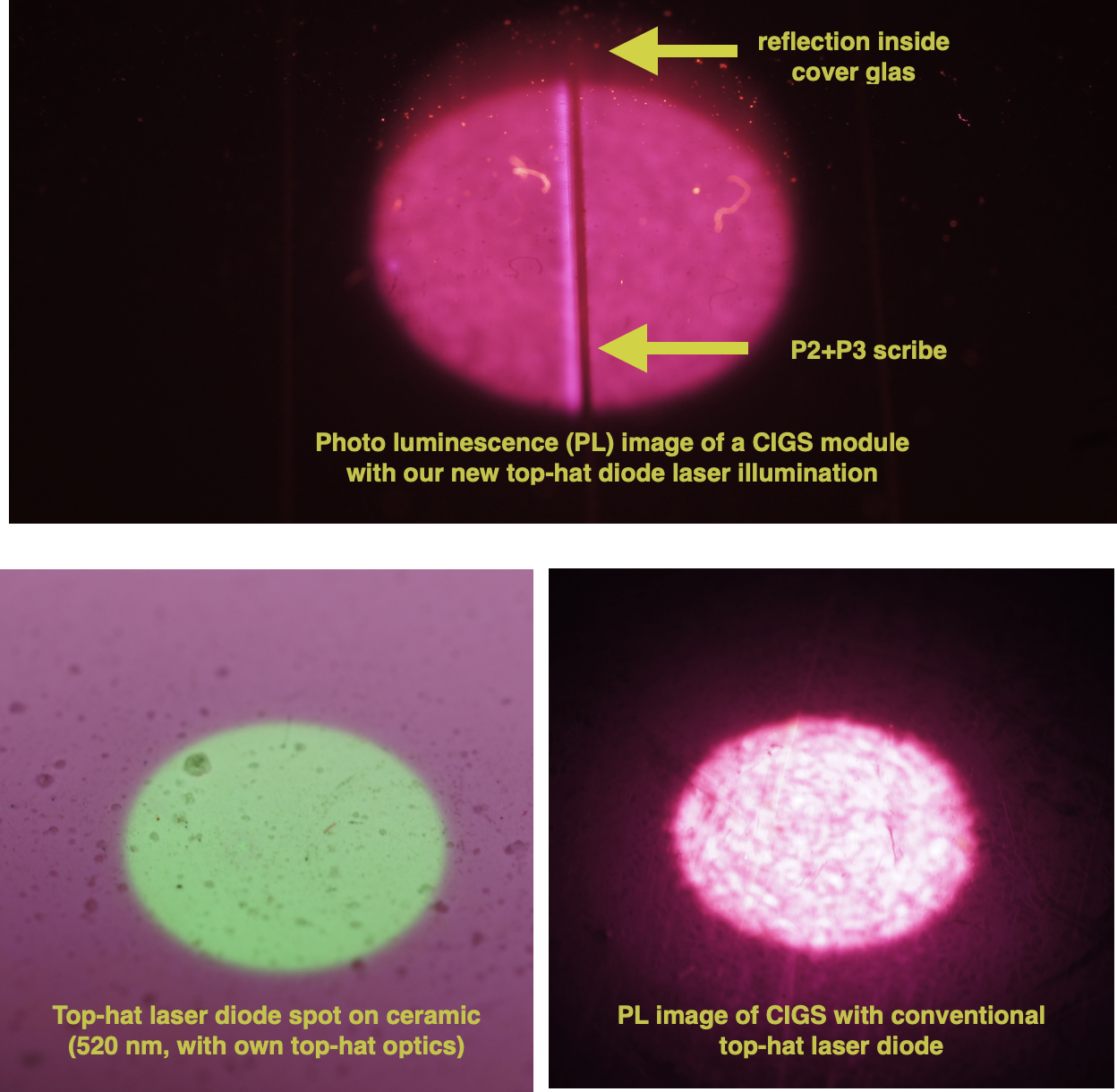
Photoluminescence image of perovskite layers illuminated with one of our top hat laser diode modules. The picture is taken with the camera build in our PEROLAS laser patterning systems