Image AI generated

Image AI generated
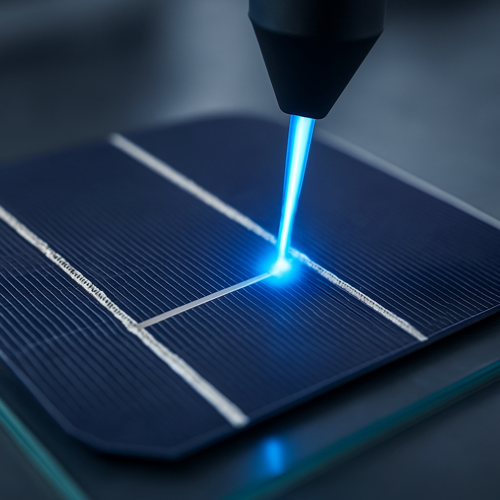
Image AI generated
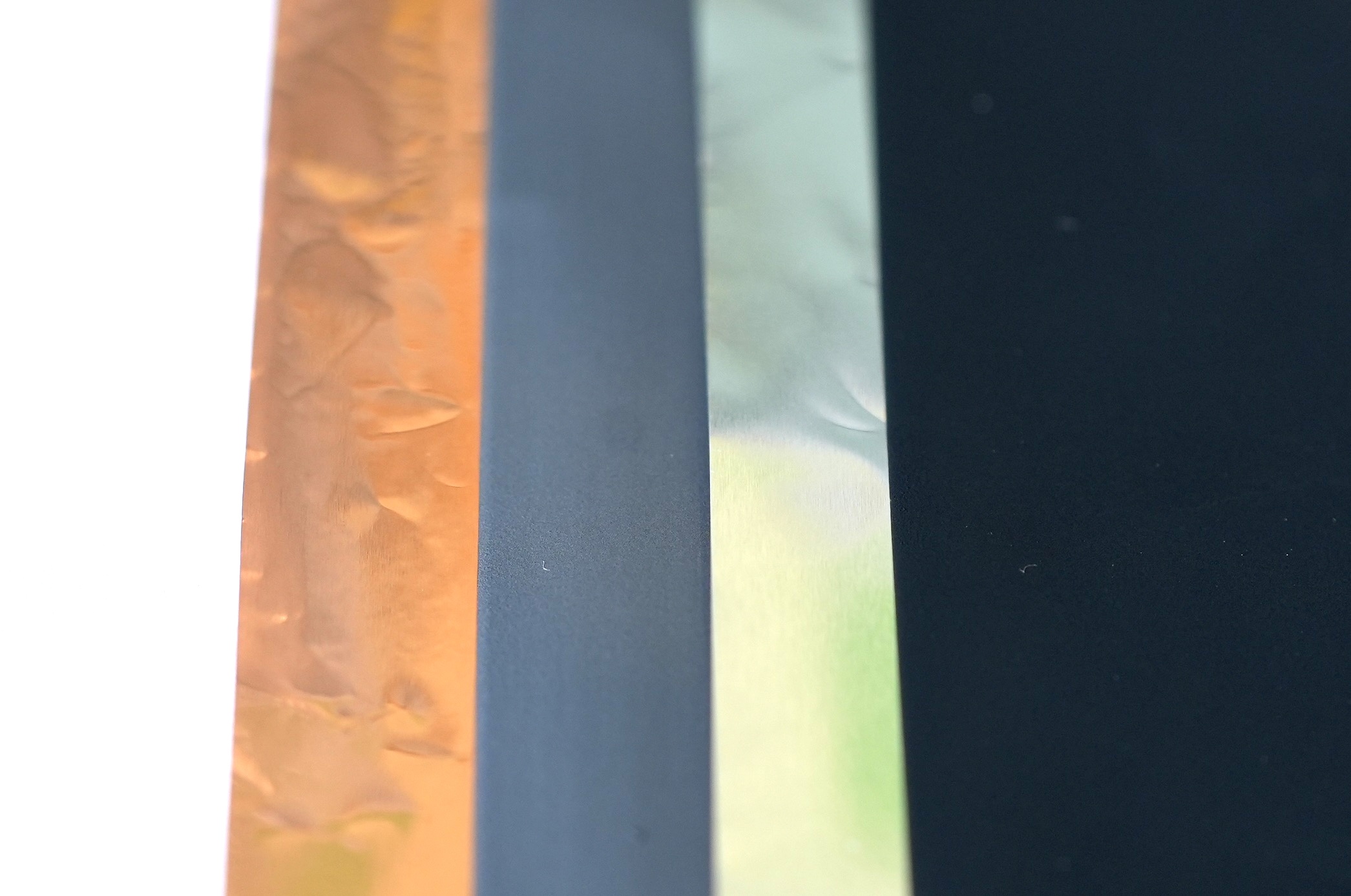
For battery anodes and cathodes
Click on image to see youtube video
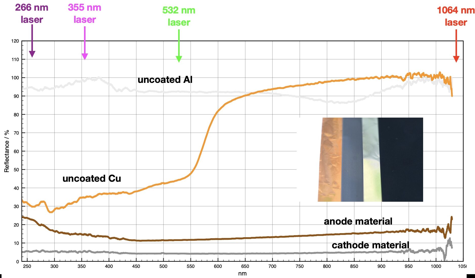
Material selective laser processing by choosing the right wavelength and pulse duration

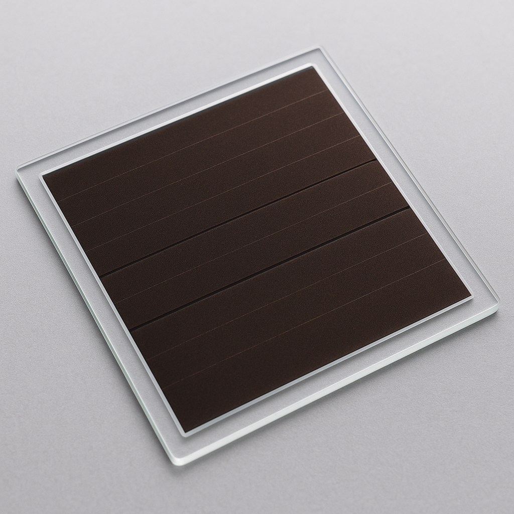
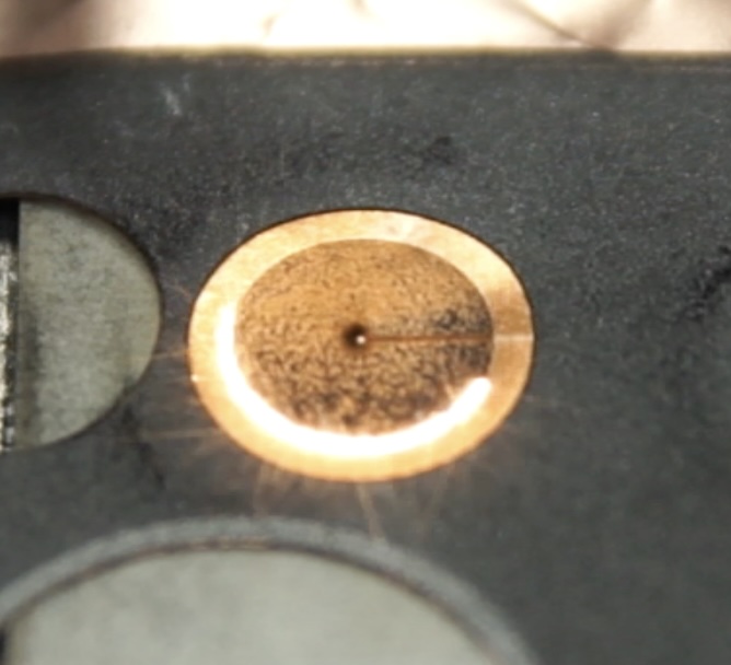
Stress-free laser cutting
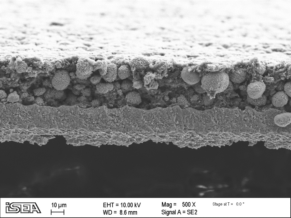
Stress-free laser cutting and electrical separation

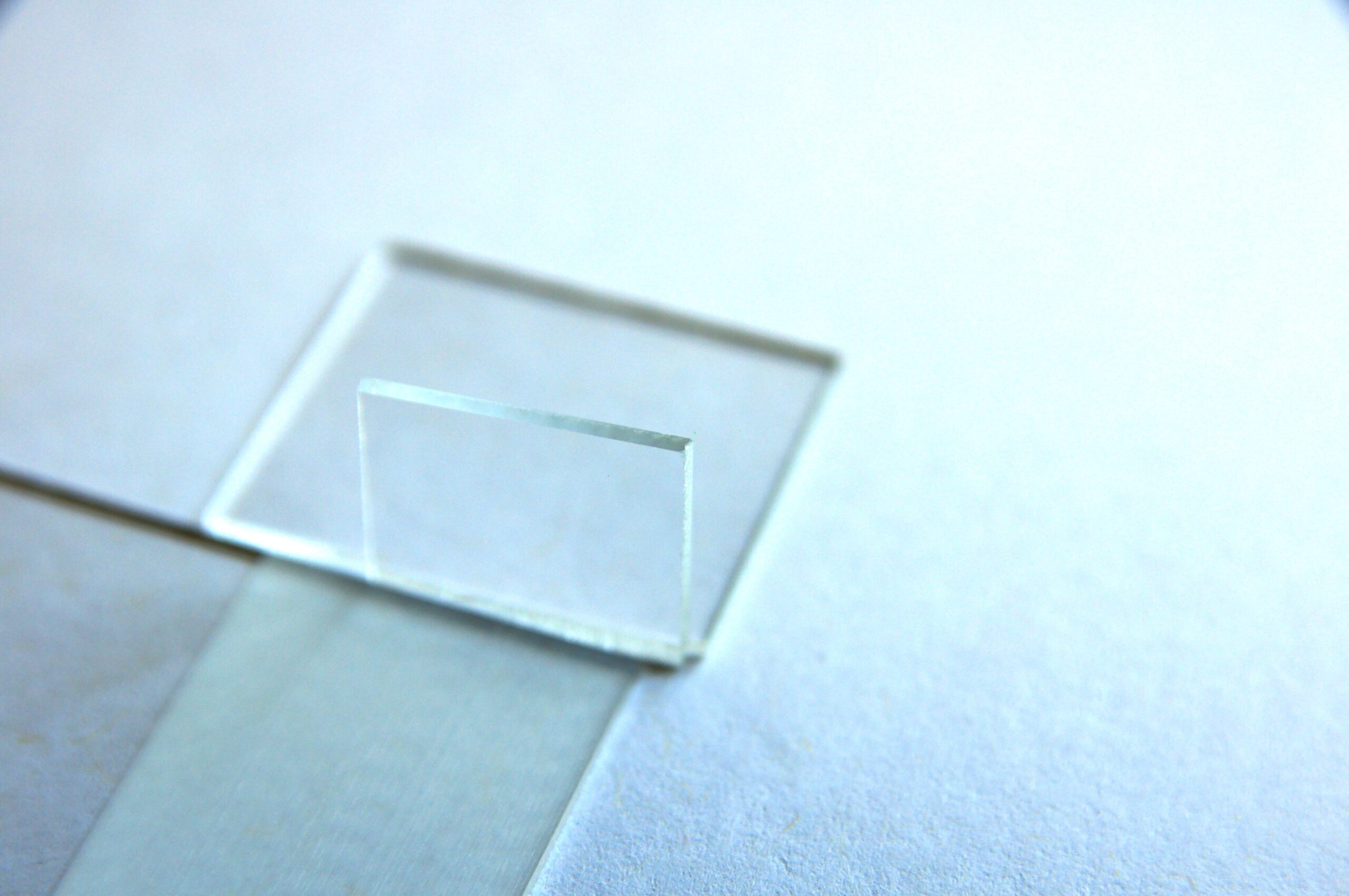
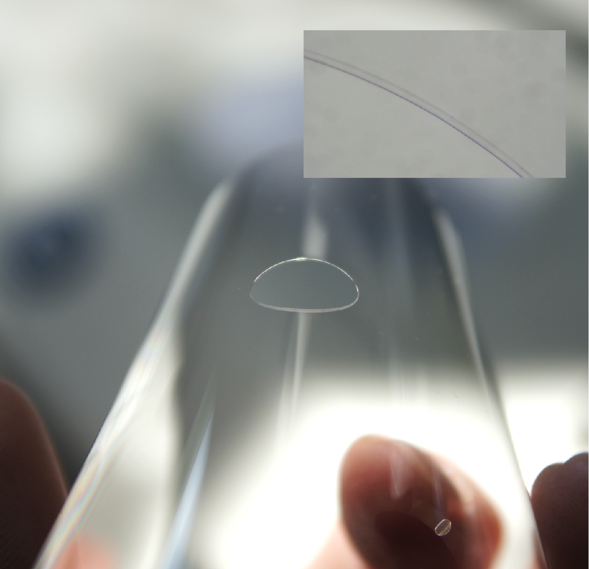
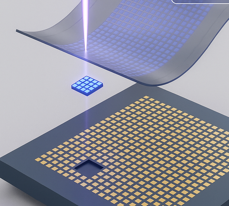
Image AI generated